Epitaxy of a crystalline layer on a crystalline substrate is widely employed to produce semiconductor heterostructures and is extremely important nowadays for the production of functional semiconductor devices. However, high substrate costs and thermal or lattice mismatch of the substrate and epitaxial layer material often limits the fabrication of more variable devices.
Recently, remote epitaxy was proposed as an advanced semiconductor manufacturing technique that allows the growth of high-quality single-crystal films on a substrate while enabling the easy separation of the grown layer from the substrate. Remote epitaxy typically relies on graphene – a single layer of connected carbon atoms - that is transferred onto the substrate prior to growth and acts like an extremely thin separator between film and substrate. However, current approaches require manual transfer of graphene or high-temperature direct growth. However, this significantly complicates and limits the application of remote epitaxy.
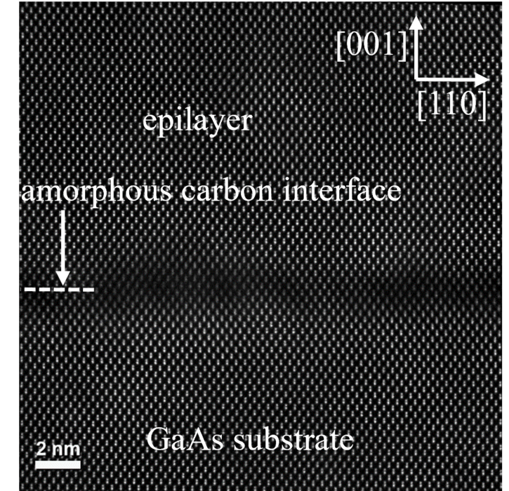
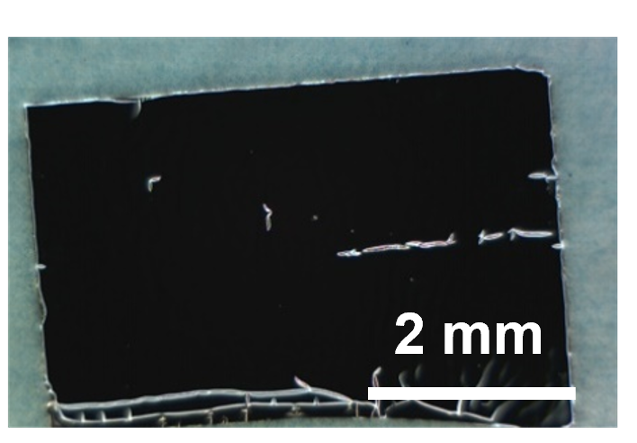
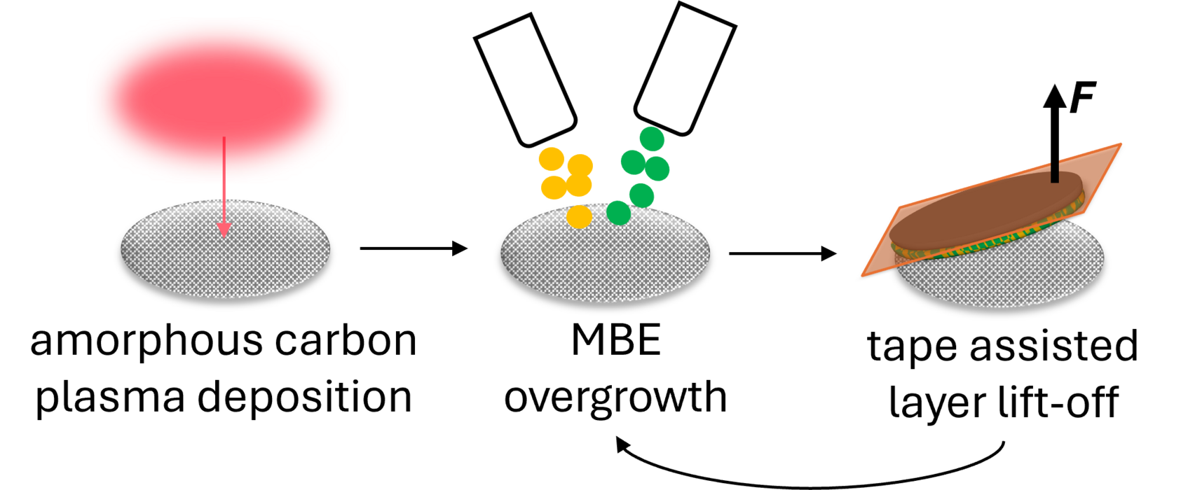
Researchers from the Paderborn University now developed a new method using ultra-thin amorphous carbon films which mimic the extremely thin graphene sheet, and which can be used as a universal template for remote epitaxy. The researchers used plasma-enhanced chemical vapor deposition technique to create smooth ultra-thin amorphous carbon layers on III-V semiconductor substrates like GaAs or InP. High quality growth and epitaxial film lift-off from the substrate was demonstrated paving the way for the fabrication of freestanding versatile semiconductor structures. A key advantage of the discussed method is the compatibility with temperature-sensitive substrates, such as GaAs and InP, which are commonly used in optoelectronic and photonic devices. Additionally, the study confirms that the a-C layer remains intact after layer lift-off, meaning that substrates can be reused multiple times, significantly lowering manufacturing costs.
Overall, this work presents a cost-effective, scalable alternative for semiconductor heterostructure fabrication. It has potential applications in optoelectronics, flexible electronics, and advanced photonic devices, paving the way for more efficient and sustainable semiconductor manufacturing.
https://doi.org/10.1038/s43246-024-00718-7
Autoren: T. Henksmeier, P. Mahler, A.Wolff, D. Deutsch, M. Voigt, L.Ruhm, A.M. Sanchez, D. J. As, G. Grundmeier, D. Reuter

